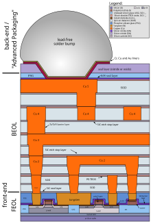
The front end of line (FEOL) is the first portion of IC fabrication where the individual components (transistors, capacitors, resistors, etc.) are patterned in a semiconductor substrate.[1] FEOL generally covers everything up to (but not including) the deposition of metal interconnect layers.[2]


Steps
For the CMOS process, FEOL contains all fabrication steps needed to form isolated CMOS elements:[3][4]
- Selecting the type of wafer to be used; Chemical-mechanical planarization (CMP) and cleaning of the wafer.
- Shallow trench isolation (STI) (or LOCOS in early processes with feature size > 0.25 μm);
- Well formation;
- Gate module formation;
- Source and drain module formation.
Finally, the surface is treated to prepare the contacts for the subsequent metallization. This concludes the FEOL process, that is, all devices have been built.[4]
Following these steps, the devices must be connected electrically as per the nets to build the electrical circuit. This is done in the back end of line (BEOL). BEOL is thus the second portion of IC fabrication where the individual devices are connected.[4]
See also
References
Further reading
- "CMOS: Circuit Design, Layout, and Simulation" Wiley-IEEE, 2010. ISBN 978-0-470-88132-3. pages 177-178 (Chapter 7.2 CMOS Process Integration); pages 180-199 (7.2.1 Frontend-of-the-line integration)
- "Fundamentals of Layout Design for Electronic Circuits", by Lienig, Scheible, Springer, doi:10.1007/978-3-030-39284-0ISBN 978-3-030-39284-0, 2020. Chapter 2: Technology Know-How: From Silicon to Devices, pages 78-82 (2.9.3 FEOL: Creating Devices)