Moore's law is the observation that the number of transistors in an integrated circuit (IC) doubles about every two years. Moore's law is an observation and projection of a historical trend. Rather than a law of physics, it is an empirical relationship linked to gains from experience in production.

The observation is named after Gordon Moore, the co-founder of Fairchild Semiconductor and Intel (and former CEO of the latter), who in 1965 posited a doubling every year in the number of components per integrated circuit,[a] and projected this rate of growth would continue for at least another decade. In 1975, looking forward to the next decade, he revised the forecast to doubling every two years, a compound annual growth rate (CAGR) of 41%. While Moore did not use empirical evidence in forecasting that the historical trend would continue, his prediction has held since 1975 and has since become known as a "law".
Moore's prediction has been used in the semiconductor industry to guide long-term planning and to set targets for research and development, thus functioning to some extent as a self-fulfilling prophecy. Advancements in digital electronics, such as the reduction in quality-adjusted microprocessor prices, the increase in memory capacity (RAM and flash), the improvement of sensors, and even the number and size of pixels in digital cameras, are strongly linked to Moore's law. These ongoing changes in digital electronics have been a driving force of technological and social change, productivity, and economic growth.
Industry experts have not reached a consensus on exactly when Moore's law will cease to apply. Microprocessor architects report that semiconductor advancement has slowed industry-wide since around 2010, slightly below the pace predicted by Moore's law. In September 2022, Nvidia CEO Jensen Huang considered Moore's law dead,[2] while Intel CEO Pat Gelsinger was of the opposite view.[3]
History
In 1959, Douglas Engelbart studied the projected downscaling of integrated circuit (IC) size, publishing his results in the article "Microelectronics, and the Art of Similitude".[4][5][6] Engelbart presented his findings at the 1960 International Solid-State Circuits Conference, where Moore was present in the audience.[7]
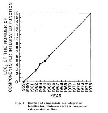
In 1965, Gordon Moore, who at the time was working as the director of research and development at Fairchild Semiconductor, was asked to contribute to the thirty-fifth anniversary issue of Electronics magazine with a prediction on the future of the semiconductor components industry over the next ten years.[8] His response was a brief article entitled "Cramming more components onto integrated circuits".[1][9][b] Within his editorial, he speculated that by 1975 it would be possible to contain as many as 65,000 components on a single quarter-square-inch (~1.6 square-centimeter) semiconductor.
The complexity for minimum component costs has increased at a rate of roughly a factor of two per year. Certainly over the short term this rate can be expected to continue, if not to increase. Over the longer term, the rate of increase is a bit more uncertain, although there is no reason to believe it will not remain nearly constant for at least 10 years.[1]
Moore posited a log-linear relationship between device complexity (higher circuit density at reduced cost) and time.[12][13] In a 2015 interview, Moore noted of the 1965 article: "...I just did a wild extrapolation saying it's going to continue to double every year for the next 10 years."[14] One historian of the law cites Stigler's law of eponymy, to introduce the fact that the regular doubling of components was known to many working in the field.[13]
In 1974, Robert H. Dennard at IBM recognized the rapid MOSFET scaling technology and formulated what became known as Dennard scaling, which describes that as MOS transistors get smaller, their power density stays constant such that the power use remains in proportion with area.[15][16] Evidence from the semiconductor industry shows that this inverse relationship between power density and areal density broke down in the mid-2000s.[17]
At the 1975 IEEE International Electron Devices Meeting, Moore revised his forecast rate,[18][19] predicting semiconductor complexity would continue to double annually until about 1980, after which it would decrease to a rate of doubling approximately every two years.[19][20][21] He outlined several contributing factors for this exponential behavior:[12][13]
- The advent of metal–oxide–semiconductor (MOS) technology
- The exponential rate of increase in die sizes, coupled with a decrease in defective densities, with the result that semiconductor manufacturers could work with larger areas without losing reduction yields
- Finer minimum dimensions
- What Moore called "circuit and device cleverness"
Shortly after 1975, Caltech professor Carver Mead popularized the term "Moore's law".[22][23] Moore's law eventually came to be widely accepted as a goal for the semiconductor industry, and it was cited by competitive semiconductor manufacturers as they strove to increase processing power. Moore viewed his eponymous law as surprising and optimistic: "Moore's law is a violation of Murphy's law. Everything gets better and better."[24] The observation was even seen as a self-fulfilling prophecy.[25][26]
The doubling period is often misquoted as 18 months because of a separate prediction by Moore's colleague, Intel executive David House.[27] In 1975, House noted that Moore's revised law of doubling transistor count every 2 years in turn implied that computer chip performance would roughly double every 18 months[28] (with no increase in power consumption).[29] Mathematically, Moore's law predicted that transistor count would double every 2 years due to shrinking transistor dimensions and other improvements.[30] As a consequence of shrinking dimensions, Dennard scaling predicted that power consumption per unit area would remain constant. Combining these effects, David House deduced that computer chip performance would roughly double every 18 months. Also due to Dennard scaling, this increased performance would not be accompanied by increased power, i.e., the energy-efficiency of silicon-based computer chips roughly doubles every 18 months. Dennard scaling ended in the 2000s.[17] Koomey later showed that a similar rate of efficiency improvement predated silicon chips and Moore's law, for technologies such as vacuum tubes.
.jpg)
Microprocessor architects report that since around 2010, semiconductor advancement has slowed industry-wide below the pace predicted by Moore's law.[17] Brian Krzanich, the former CEO of Intel, cited Moore's 1975 revision as a precedent for the current deceleration, which results from technical challenges and is "a natural part of the history of Moore's law".[31][32][33] The rate of improvement in physical dimensions known as Dennard scaling also ended in the mid-2000s. As a result, much of the semiconductor industry has shifted its focus to the needs of major computing applications rather than semiconductor scaling.[25][34][17] Nevertheless, leading semiconductor manufacturers TSMC and Samsung Electronics have claimed to keep pace with Moore's law[35][36][37][38][39][40] with 10, 7, and 5 nm nodes in mass production.[35][36][41][42][43]
Moore's second law
As the cost of computer power to the consumer falls, the cost for producers to fulfill Moore's law follows an opposite trend: R&D, manufacturing, and test costs have increased steadily with each new generation of chips. Rising manufacturing costs are an important consideration for the sustaining of Moore's law.[44] This led to the formulation of Moore's second law, also called Rock's law (named after Arthur Rock), which is that the capital cost of a semiconductor fabrication plant also increases exponentially over time.[45][46]
Major enabling factors

Numerous innovations by scientists and engineers have sustained Moore's law since the beginning of the IC era. Some of the key innovations are listed below, as examples of breakthroughs that have advanced integrated circuit and semiconductor device fabrication technology, allowing transistor counts to grow by more than seven orders of magnitude in less than five decades.
- Integrated circuit (IC): The raison d'être for Moore's law. The germanium hybrid IC was invented by Jack Kilby at Texas Instruments in 1958,[47] followed by the invention of the silicon monolithic IC chip by Robert Noyce at Fairchild Semiconductor in 1959.[48]
- Complementary metal–oxide–semiconductor (CMOS): The CMOS process was invented by Chih-Tang Sah and Frank Wanlass at Fairchild Semiconductor in 1963.[49][50][51]
- Dynamic random-access memory (DRAM): DRAM was developed by Robert H. Dennard at IBM in 1967.[52]
- Chemically amplified photoresist: Invented by Hiroshi Ito, C. Grant Willson and J. M. J. Fréchet at IBM circa 1980,[53][54][55] which was 5–10 times more sensitive to ultraviolet light.[56] IBM introduced chemically amplified photoresist for DRAM production in the mid-1980s.[57][58]
- Deep UV excimer laser photolithography: Invented by Kanti Jain[59] at IBM circa 1980.[60][61][62] Prior to this, excimer lasers had been mainly used as research devices since their development in the 1970s.[63][64] From a broader scientific perspective, the invention of excimer laser lithography has been highlighted as one of the major milestones in the 50-year history of the laser.[65][66]
- Interconnect innovations: Interconnect innovations of the late 1990s, including chemical-mechanical polishing or chemical mechanical planarization (CMP), trench isolation, and copper interconnects—although not directly a factor in creating smaller transistors—have enabled improved wafer yield, additional layers of metal wires, closer spacing of devices, and lower electrical resistance.[67][68][69]
Computer industry technology road maps predicted in 2001 that Moore's law would continue for several generations of semiconductor chips.[70]
Recent trends

One of the key technical challenges of engineering future nanoscale transistors is the design of gates. As device dimension shrinks, controlling the current flow in the thin channel becomes more difficult. Modern nanoscale transistors typically take the form of multi-gate MOSFETs, with the FinFET being the most common nanoscale transistor. The FinFET has gate dielectric on three sides of the channel. In comparison, the gate-all-around MOSFET (GAAFET) structure has even better gate control.
- A gate-all-around MOSFET (GAAFET) was first demonstrated in 1988, by a Toshiba research team led by Fujio Masuoka, who demonstrated a vertical nanowire GAAFET which he called a "surrounding gate transistor" (SGT).[71][72] Masuoka, best known as the inventor of flash memory, later left Toshiba and founded Unisantis Electronics in 2004 to research surrounding-gate technology along with Tohoku University.[73]
- In 2006, a team of Korean researchers from the Korea Advanced Institute of Science and Technology (KAIST) and the National Nano Fab Center developed a 3 nm transistor, the world's smallest nanoelectronic device at the time, based on FinFET technology.[74][75]
- In 2010, researchers at the Tyndall National Institute in Cork, Ireland announced a junctionless transistor. A control gate wrapped around a silicon nanowire can control the passage of electrons without the use of junctions or doping. They claim these may be produced at 10-nm scale using existing fabrication techniques.[76]
- In 2011, researchers at the University of Pittsburgh announced the development of a single-electron transistor, 1.5 nm in diameter, made out of oxide-based materials. Three "wires" converge on a central "island" that can house one or two electrons. Electrons tunnel from one wire to another through the island. Conditions on the third wire result in distinct conductive properties including the ability of the transistor to act as a solid state memory.[77] Nanowire transistors could spur the creation of microscopic computers.[78][79][80]
- In 2012, a research team at the University of New South Wales announced the development of the first working transistor consisting of a single atom placed precisely in a silicon crystal (not just picked from a large sample of random transistors).[81] Moore's law predicted this milestone to be reached for ICs in the lab by 2020.
- In 2015, IBM demonstrated 7 nm node chips with silicon-germanium transistors produced using EUVL. The company believed this transistor density would be four times that of the then current 14 nm chips.[82]
- Samsung and TSMC plan to manufacture 3 nm GAAFET nodes by 2021–2022.[83][84] Note that node names, such as 3 nm, have no relation to the physical size of device elements (transistors).
- A Toshiba research team including T. Imoto, M. Matsui and C. Takubo developed a "System Block Module" wafer bonding process for manufacturing three-dimensional integrated circuit (3D IC) packages in 2001.[85][86] In April 2007, Toshiba introduced an eight-layer 3D IC, the 16 GB THGAM embedded NAND flash memory chip which was manufactured with eight stacked 2 GB NAND flash chips.[87] In September 2007, Hynix introduced 24-layer 3D IC, a 16 GB flash memory chip that was manufactured with 24 stacked NAND flash chips using a wafer bonding process.[88]
- V-NAND, also known as 3D NAND, allows flash memory cells to be stacked vertically using charge trap flash technology originally presented by John Szedon in 1967, significantly increasing the number of transistors on a flash memory chip. 3D NAND was first announced by Toshiba in 2007.[89] V-NAND was first commercially manufactured by Samsung Electronics in 2013.[90][91][92]
- In 2008, researchers at HP Labs announced a working memristor, a fourth basic passive circuit element whose existence only had been theorized previously. The memristor's unique properties permit the creation of smaller and better-performing electronic devices.[93]
- In 2014, bioengineers at Stanford University developed a circuit modeled on the human brain. Sixteen "Neurocore" chips simulate one million neurons and billions of synaptic connections, claimed to be 9,000 times faster as well as more energy efficient than a typical PC.[94]
- In 2015, Intel and Micron announced 3D XPoint, a non-volatile memory claimed to be significantly faster with similar density compared to NAND. Production scheduled to begin in 2016 was delayed until the second half of 2017.[95][96][97]
- In 2017, Samsung combined its V-NAND technology with eUFS 3D IC stacking to produce a 512 GB flash memory chip, with eight stacked 64-layer V-NAND dies.[98] In 2019, Samsung produced a 1 TB flash chip with eight stacked 96-layer V-NAND dies, along with quad-level cell (QLC) technology (4-bit per transistor),[99][100] equivalent to 2 trillion transistors, the highest transistor count of any IC chip.
- In 2020, Samsung Electronics planned to produce the 5 nm node, using FinFET and EUV technology.[36][needs update]
- In May 2021, IBM announced the creation of the first 2 nm computer chip, with parts supposedly being smaller than human DNA.[101]
Microprocessor architects report that semiconductor advancement has slowed industry-wide since around 2010, below the pace predicted by Moore's law.[17] Brian Krzanich, the former CEO of Intel, announced, "Our cadence today is closer to two and a half years than two."[102] Intel stated in 2015 that improvements in MOSFET devices have slowed, starting at the 22 nm feature width around 2012, and continuing at 14 nm.[103]
The physical limits to transistor scaling have been reached due to source-to-drain leakage, limited gate metals and limited options for channel material. Other approaches are being investigated, which do not rely on physical scaling. These include the spin state of electron spintronics, tunnel junctions, and advanced confinement of channel materials via nano-wire geometry.[104] Spin-based logic and memory options are being developed actively in labs.[105][106]
Alternative materials research
The vast majority of current transistors on ICs are composed principally of doped silicon and its alloys. As silicon is fabricated into single nanometer transistors, short-channel effects adversely change desired material properties of silicon as a functional transistor. Below are several non-silicon substitutes in the fabrication of small nanometer transistors.
One proposed material is indium gallium arsenide, or InGaAs. Compared to their silicon and germanium counterparts, InGaAs transistors are more promising for future high-speed, low-power logic applications. Because of intrinsic characteristics of III-V compound semiconductors, quantum well and tunnel effect transistors based on InGaAs have been proposed as alternatives to more traditional MOSFET designs.
- In the early 2000s, the atomic layer deposition high-κ film and pitch double-patterning processes were invented by Gurtej Singh Sandhu at Micron Technology, extending Moore's law for planar CMOS technology to 30 nm class and smaller.
- In 2009, Intel announced the development of 80-nm InGaAs quantum well transistors. Quantum well devices contain a material sandwiched between two layers of material with a wider band gap. Despite being double the size of leading pure silicon transistors at the time, the company reported that they performed equally as well while consuming less power.[107]
- In 2011, researchers at Intel demonstrated 3-D tri-gate InGaAs transistors with improved leakage characteristics compared to traditional planar designs. The company claims that their design achieved the best electrostatics of any III-V compound semiconductor transistor.[108] At the 2015 International Solid-State Circuits Conference, Intel mentioned the use of III-V compounds based on such an architecture for their 7 nm node.[109][110]
- In 2011, researchers at the University of Texas at Austin developed an InGaAs tunneling field-effect transistors capable of higher operating currents than previous designs. The first III-V TFET designs were demonstrated in 2009 by a joint team from Cornell University and Pennsylvania State University.[111][112]
- In 2012, a team in MIT's Microsystems Technology Laboratories developed a 22 nm transistor based on InGaAs which, at the time, was the smallest non-silicon transistor ever built. The team used techniques used in silicon device fabrication and aimed for better electrical performance and a reduction to 10-nanometer scale.[113]
Biological computing research shows that biological material has superior information density and energy efficiency compared to silicon-based computing.[114]

Various forms of graphene are being studied for graphene electronics, e.g. graphene nanoribbon transistors have shown promise since its appearance in publications in 2008. (Bulk graphene has a band gap of zero and thus cannot be used in transistors because of its constant conductivity, an inability to turn off. The zigzag edges of the nanoribbons introduce localized energy states in the conduction and valence bands and thus a bandgap that enables switching when fabricated as a transistor. As an example, a typical GNR of width of 10 nm has a desirable bandgap energy of 0.4 eV.[115][116]) More research will need to be performed, however, on sub-50 nm graphene layers, as its resistivity value increases and thus electron mobility decreases.[115]
Forecasts and roadmaps
In April 2005, Gordon Moore stated in an interview that the projection cannot be sustained indefinitely: "It can't continue forever. The nature of exponentials is that you push them out and eventually disaster happens." He also noted that transistors eventually would reach the limits of miniaturization at atomic levels:
In terms of size [of transistors] you can see that we're approaching the size of atoms which is a fundamental barrier, but it'll be two or three generations before we get that far—but that's as far out as we've ever been able to see. We have another 10 to 20 years before we reach a fundamental limit. By then they'll be able to make bigger chips and have transistor budgets in the billions.[117]
— Gordon Moore
In 2016 the International Technology Roadmap for Semiconductors, after using Moore's Law to drive the industry since 1998, produced its final roadmap. It no longer centered its research and development plan on Moore's law. Instead, it outlined what might be called the More than Moore strategy in which the needs of applications drive chip development, rather than a focus on semiconductor scaling. Application drivers range from smartphones to AI to data centers.[118]
IEEE began a road-mapping initiative in 2016, "Rebooting Computing", named the International Roadmap for Devices and Systems (IRDS).[119]
Some forecasters, including Gordon Moore,[120] predict that Moore's law will end by around 2025.[121][118][122] Although Moore's Law will reach a physical limit, some forecasters are optimistic about the continuation of technological progress in a variety of other areas, including new chip architectures, quantum computing, and AI and machine learning.[123][124] Nvidia CEO Jensen Huang declared Moore's law dead in 2022;[2] several days later, Intel CEO Pat Gelsinger countered with the opposite claim.[3]
Consequences
Digital electronics have contributed to world economic growth in the late twentieth and early twenty-first centuries.[125] The primary driving force of economic growth is the growth of productivity,[126] which Moore's law factors into. Moore (1995) expected that "the rate of technological progress is going to be controlled from financial realities".[127] The reverse could and did occur around the late-1990s, however, with economists reporting that "Productivity growth is the key economic indicator of innovation."[128] Moore's law describes a driving force of technological and social change, productivity, and economic growth.[129][130][126]
An acceleration in the rate of semiconductor progress contributed to a surge in U.S. productivity growth,[131][132][133] which reached 3.4% per year in 1997–2004, outpacing the 1.6% per year during both 1972–1996 and 2005–2013.[134] As economist Richard G. Anderson notes, "Numerous studies have traced the cause of the productivity acceleration to technological innovations in the production of semiconductors that sharply reduced the prices of such components and of the products that contain them (as well as expanding the capabilities of such products)."[135]
The primary negative implication of Moore's law is that obsolescence pushes society up against the Limits to Growth. As technologies continue to rapidly "improve", they render predecessor technologies obsolete. In situations in which security and survivability of hardware or data are paramount, or in which resources are limited, rapid obsolescence often poses obstacles to smooth or continued operations.[136]
Because of the intensive resource footprint and toxic materials used in the production of computers, obsolescence leads to serious harmful environmental impacts. Americans throw out 400,000 cell phones every day,[137] but this high level of obsolescence appears to companies as an opportunity to generate regular sales of expensive new equipment, instead of retaining one device for a longer period of time, leading to industry using planned obsolescence as a profit centre.[138]

An alternative source of improved performance is in microarchitecture techniques exploiting the growth of available transistor count. Out-of-order execution and on-chip caching and prefetching reduce the memory latency bottleneck at the expense of using more transistors and increasing the processor complexity. These increases are described empirically by Pollack's Rule, which states that performance increases due to microarchitecture techniques approximate the square root of the complexity (number of transistors or the area) of a processor.[139]
For years, processor makers delivered increases in clock rates and instruction-level parallelism, so that single-threaded code executed faster on newer processors with no modification.[140] Now, to manage CPU power dissipation, processor makers favor multi-core chip designs, and software has to be written in a multi-threaded manner to take full advantage of the hardware. Many multi-threaded development paradigms introduce overhead, and will not see a linear increase in speed versus number of processors. This is particularly true while accessing shared or dependent resources, due to lock contention. This effect becomes more noticeable as the number of processors increases. There are cases where a roughly 45% increase in processor transistors has translated to roughly 10–20% increase in processing power.[141]
On the other hand, manufacturers are adding specialized processing units to deal with features such as graphics, video, and cryptography. For one example, Intel's Parallel JavaScript extension not only adds support for multiple cores, but also for the other non-general processing features of their chips, as part of the migration in client side scripting toward HTML5.[142]
Moore's law has affected the performance of other technologies significantly: Michael S. Malone wrote of a Moore's War following the apparent success of shock and awe in the early days of the Iraq War. Progress in the development of guided weapons depends on electronic technology.[143] Improvements in circuit density and low-power operation associated with Moore's law also have contributed to the development of technologies including mobile telephones[144] and 3-D printing.[145]
Other formulations and similar observations
Several measures of digital technology are improving at exponential rates related to Moore's law, including the size, cost, density, and speed of components. Moore wrote only about the density of components, "a component being a transistor, resistor, diode or capacitor",[127] at minimum cost.
Transistors per integrated circuit – The most popular formulation is of the doubling of the number of transistors on ICs every two years. At the end of the 1970s, Moore's law became known as the limit for the number of transistors on the most complex chips. The graph at the top of this article shows this trend holds true today. As of 2017[update], the commercially available processor possessing the highest number of transistors is the 48 core Centriq with over 18 billion transistors.[146]
Density at minimum cost per transistor
This is the formulation given in Moore's 1965 paper.[1] It is not just about the density of transistors that can be achieved, but about the density of transistors at which the cost per transistor is the lowest.[147]
As more transistors are put on a chip, the cost to make each transistor decreases, but the chance that the chip will not work due to a defect increases. In 1965, Moore examined the density of transistors at which cost is minimized, and observed that, as transistors were made smaller through advances in photolithography, this number would increase at "a rate of roughly a factor of two per year".[1]
Dennard scaling – This posits that power usage would decrease in proportion to area (both voltage and current being proportional to length) of transistors. Combined with Moore's law, performance per watt would grow at roughly the same rate as transistor density, doubling every 1–2 years. According to Dennard scaling transistor dimensions would be scaled by 30% (0.7x) every technology generation, thus reducing their area by 50%. This would reduce the delay by 30% (0.7x) and therefore increase operating frequency by about 40% (1.4x). Finally, to keep electric field constant, voltage would be reduced by 30%, reducing energy by 65% and power (at 1.4x frequency) by 50%.[c] Therefore, in every technology generation transistor density would double, circuit becomes 40% faster, while power consumption (with twice the number of transistors) stays the same.[148] Dennard scaling ended in 2005–2010, due to leakage currents.[17]
The exponential processor transistor growth predicted by Moore does not always translate into exponentially greater practical CPU performance. Since around 2005–2007, Dennard scaling has ended, so even though Moore's law continued after that, it has not yielded proportional dividends in improved performance.[15][149] The primary reason cited for the breakdown is that at small sizes, current leakage poses greater challenges, and also causes the chip to heat up, which creates a threat of thermal runaway and therefore, further increases energy costs.[15][149][17]
The breakdown of Dennard scaling prompted a greater focus on multicore processors, but the gains offered by switching to more cores are lower than the gains that would be achieved had Dennard scaling continued.[150][151] In another departure from Dennard scaling, Intel microprocessors adopted a non-planar tri-gate FinFET at 22 nm in 2012 that is faster and consumes less power than a conventional planar transistor.[152] The rate of performance improvement for single-core microprocessors has slowed significantly.[153] Single-core performance was improving by 52% per year in 1986–2003 and 23% per year in 2003–2011, but slowed to just seven percent per year in 2011–2018.[153]
Quality adjusted price of IT equipment – The price of information technology (IT), computers and peripheral equipment, adjusted for quality and inflation, declined 16% per year on average over the five decades from 1959 to 2009.[154][155] The pace accelerated, however, to 23% per year in 1995–1999 triggered by faster IT innovation,[128] and later, slowed to 2% per year in 2010–2013.[154][156]
While quality-adjusted microprocessor price improvement continues,[157] the rate of improvement likewise varies, and is not linear on a log scale. Microprocessor price improvement accelerated during the late 1990s, reaching 60% per year (halving every nine months) versus the typical 30% improvement rate (halving every two years) during the years earlier and later.[158][159] Laptop microprocessors in particular improved 25–35% per year in 2004–2010, and slowed to 15–25% per year in 2010–2013.[160]
The number of transistors per chip cannot explain quality-adjusted microprocessor prices fully.[158][161][162] Moore's 1995 paper does not limit Moore's law to strict linearity or to transistor count, "The definition of 'Moore's Law' has come to refer to almost anything related to the semiconductor industry that on a semi-log plot approximates a straight line. I hesitate to review its origins and by doing so restrict its definition."[127]
Hard disk drive areal density – A similar prediction (sometimes called Kryder's law) was made in 2005 for hard disk drive areal density.[163] The prediction was later viewed as over-optimistic. Several decades of rapid progress in areal density slowed around 2010, from 30 to 100% per year to 10–15% per year, because of noise related to smaller grain size of the disk media, thermal stability, and writability using available magnetic fields.[164][165]
Fiber-optic capacity – The number of bits per second that can be sent down an optical fiber increases exponentially, faster than Moore's law. Keck's law, in honor of Donald Keck.[166]
Network capacity – According to Gerald Butters,[167][168] the former head of Lucent's Optical Networking Group at Bell Labs, there is another version, called Butters' Law of Photonics,[169] a formulation that deliberately parallels Moore's law. Butters' law says that the amount of data coming out of an optical fiber is doubling every nine months.[170] Thus, the cost of transmitting a bit over an optical network decreases by half every nine months. The availability of wavelength-division multiplexing (sometimes called WDM) increased the capacity that could be placed on a single fiber by as much as a factor of 100. Optical networking and dense wavelength-division multiplexing (DWDM) is rapidly bringing down the cost of networking, and further progress seems assured. As a result, the wholesale price of data traffic collapsed in the dot-com bubble. Nielsen's Law says that the bandwidth available to users increases by 50% annually.[171]
Pixels per dollar – Similarly, Barry Hendy of Kodak Australia has plotted pixels per dollar as a basic measure of value for a digital camera, demonstrating the historical linearity (on a log scale) of this market and the opportunity to predict the future trend of digital camera price, LCD and LED screens, and resolution.[172][173][174][175]
The great Moore's law compensator (TGMLC), also known as Wirth's law – generally is referred to as software bloat and is the principle that successive generations of computer software increase in size and complexity, thereby offsetting the performance gains predicted by Moore's law. In a 2008 article in InfoWorld, Randall C. Kennedy,[176] formerly of Intel, introduces this term using successive versions of Microsoft Office between the year 2000 and 2007 as his premise. Despite the gains in computational performance during this time period according to Moore's law, Office 2007 performed the same task at half the speed on a prototypical year 2007 computer as compared to Office 2000 on a year 2000 computer.
Library expansion – was calculated in 1945 by Fremont Rider to double in capacity every 16 years, if sufficient space were made available.[177] He advocated replacing bulky, decaying printed works with miniaturized microform analog photographs, which could be duplicated on-demand for library patrons or other institutions. He did not foresee the digital technology that would follow decades later to replace analog microform with digital imaging, storage, and transmission media. Automated, potentially lossless digital technologies allowed vast increases in the rapidity of information growth in an era that now sometimes is called the Information Age.
Carlson curve – is a term coined by The Economist[178] to describe the biotechnological equivalent of Moore's law, and is named after author Rob Carlson.[179] Carlson accurately predicted that the doubling time of DNA sequencing technologies (measured by cost and performance) would be at least as fast as Moore's law.[180] Carlson Curves illustrate the rapid (in some cases hyperexponential) decreases in cost, and increases in performance, of a variety of technologies, including DNA sequencing, DNA synthesis, and a range of physical and computational tools used in protein expression and in determining protein structures.
Eroom's law – is a pharmaceutical drug development observation which was deliberately written as Moore's Law spelled backwards in order to contrast it with the exponential advancements of other forms of technology (such as transistors) over time. It states that the cost of developing a new drug roughly doubles every nine years.
Experience curve effects says that each doubling of the cumulative production of virtually any product or service is accompanied by an approximate constant percentage reduction in the unit cost. The acknowledged first documented qualitative description of this dates from 1885.[181][182] A power curve was used to describe this phenomenon in a 1936 discussion of the cost of airplanes.[183]
Edholm's law – Phil Edholm observed that the bandwidth of telecommunication networks (including the Internet) is doubling every 18 months.[184] The bandwidths of online communication networks has risen from bits per second to terabits per second. The rapid rise in online bandwidth is largely due to the same MOSFET scaling that enabled Moore's law, as telecommunications networks are built from MOSFETs.[185]
Haitz's law predicts that the brightness of LEDs increases as their manufacturing cost goes down.
Swanson's law is the observation that the price of solar photovoltaic modules tends to drop 20 percent for every doubling of cumulative shipped volume. At present rates, costs go down 75% about every 10 years.
See also
- Accelerating change – Perceived increase in the rate of technological change throughout history
- Beyond CMOS – Possible future digital logic technologies
- Ephemeralization – Technological advancement theory
- Huang's law – Computer science observation
- Koomey's law – Trend indicating the number of computations per unit energy dissipated doubles every 1.57 years
- Limits of computation – Overview of the limits of computation
- List of eponymous laws – Adages and sayings named after a person
- List of laws § Technology
- Microprocessor chronology – Timeline of microprocessor development
- Neural scaling law – Law in machine learning
- Power law – Functional relationship between two quantities
- Wirth's law – Computing adage made popular by Niklaus Wirth
Explanatory notes
References
Further reading
- Brock, David C., ed. (2006). Understanding Moore's Law: Four Decades of Innovation. Philadelphia: Chemical Heritage Foundation. ISBN 0-941901-41-6. OCLC 66463488.
- Mody, Cyrus (2016). The Long Arm of Moore's law: Microelectronics and American Science. Cambridge, Massachusetts: MIT Press. ISBN 978-0262035491.
- Thackray, Arnold; Brock, David C.; Jones, Rachel (2015). Moore's Law: The Life of Gordon Moore, Silicon Valley's Quiet Revolutionary. New York: Basic Books. ISBN 978-0-465-05564-7. OCLC 0465055648.
- Tuomi, Ilkka (November 2002). "The Lives and Death of Moore's Law". First Monday. 7 (11). doi:10.5210/fm.v7i11.1000.
External links
- Intel press kit – released for Moore's Law's 40th anniversary, with a 1965 sketch by Moore
- No Technology has been more disruptive... Slide show of microchip growth
- Intel (IA-32) CPU speeds 1994–2005 – speed increases in recent years have seemed to slow with regard to percentage increase per year (available in PDF or PNG format)
- International Technology Roadmap for Semiconductors (ITRS)
- A C|net FAQ about Moore's Law at archive.today (archived 2013-01-02)
- ASML's 'Our Stories', Gordon Moore about Moore's Law, ASML Holding
- "Why Moore's Law Matters". Asianometry. March 2023 – via YouTube.
- Moore’s Law at Intel