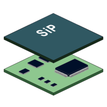
A system in a package (SiP) or system-in-package is a number of integrated circuits (ICs) enclosed in one chip carrier package or encompassing an IC package substrate that may include passive components and perform the functions of an entire system. The ICs may be stacked using package on package, placed side by side, and/or embedded in the substrate.[1] The SiP performs all or most of the functions of an electronic system, and is typically used when designing components for mobile phones, digital music players, etc.[2] Dies containing integrated circuits may be stacked vertically on the package substrate. They are internally connected by fine wires that are bonded to the package substrate. Alternatively, with a flip chip technology, solder bumps are used to join stacked chips together and to the package substrate, or even both techniques can be used in a single package. SiPs are like systems on a chip (SoCs) but less tightly integrated and not on a single semiconductor die.[3]

SIPs can be used either to reduce the size of a system, improve performance or to reduce costs.[4][5] The technology evolved from multi chip module (MCM) technology, the difference being that SiPs also use die stacking, which stacks several chips or dies on top of each other.[6][7]
Technology
SiP dies can be stacked vertically or tiled horizontally, with techniques like chiplets or quilt packaging. SiPs connect the dies with standard off-chip wire bonds or solder bumps, unlike slightly denser three-dimensional integrated circuits which connect stacked silicon dies with conductors running through the die using through-silicon vias. Many different 3D packaging techniques have been developed for stacking many fairly standard chip dies into a compact area.[8]
SiPs can contain several chips or dies—such as a specialized processor, DRAM, flash memory—combined with passive components—resistors and capacitors—all mounted on the same substrate. This means that a complete functional unit can be built in a single package, so that few external components need to be added to make it work. This is particularly valuable in space constrained environments like MP3 players and mobile phones as it reduces the complexity of the printed circuit board and overall design. Despite its benefits, this technique decreases the yield of fabrication since any defective chip in the package will result in a non-functional packaged integrated circuit, even if all other modules in that same package are functional.
SiPs are in contrast to the common system on a chip (SoC) integrated circuit architecture which integrates components based on function into a single circuit die. An SoC will typically integrate a CPU, graphics and memory interfaces, hard-disk and USB connectivity, random-access and read-only memories, and secondary storage and/or their controllers on a single die. In comparison an SiP would connect these modules as discrete components in one or more chip packages or dies. An SiP resembles the common traditional motherboard-based PC architecture, as it separates components based on function and connects them through a central interfacing circuit board. An SiP has a lower grade of integration in comparison to an SoC. Hybrid integrated circuits are somewhat similar to SiPs, however they tend to use older or less advanced technology (tend to use single layer circuit boards or substrates, not use die stacking, do not use flip chip or BGA for connecting components or dies, use only wire bonding for connecting dies or Small outline integrated circuit packages, use Dual in-line packages, or Single in-line packages for interfacing outside the Hybrid IC instead of BGA, etc.).[9]
SiP technology is primarily being driven by early market trends in wearables, mobile devices and the internet of things which do not demand the high numbers of produced units as in the established consumer and business SoC market. As the internet of things becomes more of a reality and less of a vision, there is innovation going on at the system on a chip and SiP level so that microelectromechanical (MEMS) sensors can be integrated on a separate die and control the connectivity.[10]
SiP solutions may require multiple packaging technologies, such as flip chip, wire bonding, wafer-level packaging, Through-silicon vias (TSVs), chiplets and more.[11][12]
Suppliers
- Advanced Micro Devices
- Amkor Technology
- Atmel
- AMPAK Technology Inc.
- NANIUM, S.A.
- ASE Group
- CeraMicro
- ChipSiP Technology
- Cypress Semiconductor
- STATS ChipPAC Ltd
- Toshiba
- Renesas
- SanDisk
- Samsung
- Silicon Labs
- Octavo Systems
- Nordic Semiconductor
- JCET
- Desay Sip